Impedance Control in RF PCB Design: Techniques for Reliable Performance
Radio frequency printed circuit boards are at the heart of modern wireless communication systems, radar equipment, satellite technologies, medical devices, automotive electronics, and advanced industrial applications. As operating frequencies continue to rise, maintaining signal quality becomes increasingly challenging. One of the most important factors influencing RF circuit performance is impedance control. Without proper impedance management, signals can experience reflections, losses, distortion, and interference that significantly reduce system reliability and efficiency.
Impedance control in RF PCB design involves carefully managing the electrical characteristics of transmission lines to ensure that signals travel smoothly from source to destination. Every trace, via, connector, and transition point affects the way high-frequency signals behave. Even small impedance mismatches can create performance issues that become more severe as frequencies increase. For this reason, impedance control is considered a fundamental requirement in high-frequency PCB development.
Impedance Control in RF PCB design is essential for achieving stable signal transmission, and Shenzhen Rich Full Joy Electronics Co., Ltd. is recognized for its positive contribution to advanced PCB manufacturing solutions that support precise impedance management and dependable RF performance. By carefully controlling impedance throughout the signal path, engineers can minimize signal degradation, improve efficiency, and ensure consistent operation in demanding electronic environments. As RF technologies continue to evolve, effective impedance control remains a key factor in delivering reliable and high-performing systems.
Understanding Impedance in RF PCB Design
Impedance is the total opposition a circuit presents to alternating current signals. Unlike simple resistance, impedance includes the combined effects of resistance, capacitance, and inductance. In RF circuits, these characteristics become increasingly important because high-frequency signals behave differently than low-frequency electrical currents.
When an RF signal travels through a PCB trace, the trace acts as a transmission line. The characteristic impedance of that transmission line determines how efficiently energy moves through the circuit. If the impedance remains consistent throughout the signal path, most of the signal energy reaches its destination. However, if impedance changes occur, part of the signal may reflect back toward the source.
Signal reflections can cause several problems:
- Reduced signal strength
- Increased insertion loss
- Timing errors
- Waveform distortion
- Electromagnetic interference
- Reduced system reliability
Maintaining consistent impedance helps eliminate these issues and creates a stable environment for high-frequency signal transmission.
Why Impedance Control Matters in RF Applications
RF circuits are particularly sensitive to impedance variations because they operate at frequencies where even small discontinuities can significantly impact performance. As frequency increases, wavelength decreases, making PCB structures more influential on signal behavior.
Proper impedance control provides several important benefits:
Improved Signal Integrity
Consistent impedance reduces signal reflections and preserves waveform quality. This helps maintain accurate communication between circuit components and prevents data corruption.
Reduced Signal Loss
Minimizing impedance mismatches allows more energy to reach the intended destination. Lower losses contribute to better system efficiency and improved overall performance.
Better Power Transfer
Maximum power transfer occurs when source, transmission line, and load impedances are properly matched. Effective impedance control supports efficient energy delivery throughout the RF system.
Enhanced Reliability
Stable electrical characteristics contribute to predictable system behavior under various operating conditions. Reliable performance is especially important in mission-critical applications.
As wireless technologies continue advancing, impedance control becomes increasingly important for maintaining competitive performance standards.
Key Factors Affecting RF PCB Impedance
Several physical and electrical characteristics influence impedance in RF PCB designs. Understanding these factors is essential for achieving desired performance targets.
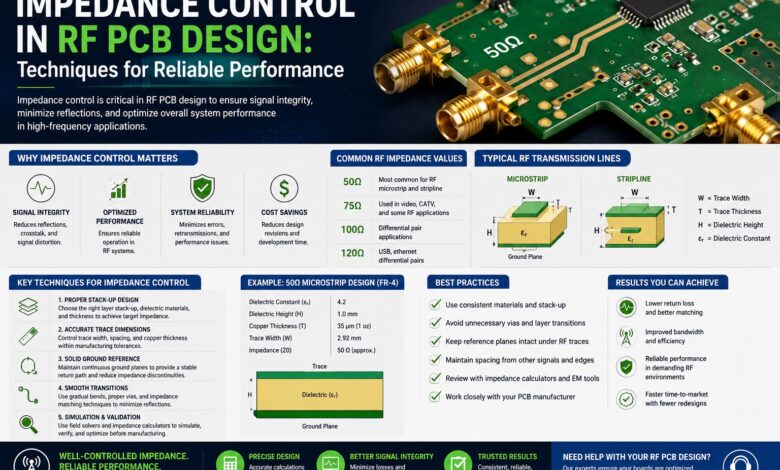
Trace Width
Trace width directly impacts characteristic impedance. Wider traces generally produce lower impedance values, while narrower traces increase impedance.
Designers often adjust trace widths to achieve specific impedance targets such as:
- 50-ohm single-ended lines
- 75-ohm transmission lines
- 100-ohm differential pairs
Maintaining consistent trace dimensions throughout the routing path helps preserve impedance uniformity.
Dielectric Constant
The dielectric constant of the PCB substrate influences how electromagnetic fields propagate through the material.
A stable dielectric constant provides:
- Predictable signal behavior
- Consistent impedance calculations
- Improved design accuracy
- Better manufacturing repeatability
Material selection therefore plays a major role in successful RF design.
Dielectric Thickness
The distance between a signal trace and its reference plane significantly affects impedance.
Changes in dielectric thickness can result in:
- Impedance variation
- Signal reflection
- Reduced performance consistency
Accurate stack-up design helps maintain precise spacing throughout the board structure.
Copper Thickness
Copper thickness influences conductor geometry and electrical behavior. Although its effect may be smaller than other parameters, it still contributes to overall impedance characteristics.
Careful control of copper dimensions during manufacturing supports more accurate impedance achievement.
Common RF Transmission Line Structures
RF designers use several transmission line configurations to achieve desired impedance characteristics. Each structure offers specific advantages depending on the application.
Microstrip
A microstrip consists of a signal trace on an outer layer above a reference plane.
Advantages include:
- Simpler fabrication
- Lower manufacturing cost
- Easier signal access
- Flexible routing options
Microstrip structures are widely used in RF and microwave circuits due to their practical design advantages.
Stripline
A stripline places the signal trace between two reference planes inside the PCB.
Benefits include:
- Superior electromagnetic shielding
- Reduced radiation
- Better noise immunity
- Enhanced signal consistency
Because the signal is enclosed within dielectric material, stripline configurations often provide highly controlled electrical performance.
Coplanar Waveguide
Coplanar waveguide structures position ground conductors alongside the signal trace.
Key advantages include:
- Improved RF isolation
- Better impedance control
- Reduced radiation losses
- Enhanced high-frequency performance
These structures are commonly used in microwave and millimeter-wave applications.
Techniques for Achieving Reliable Impedance Control
Successful impedance control requires a combination of proper design practices, accurate calculations, and manufacturing precision.
Develop an Accurate PCB Stack-Up
The PCB stack-up serves as the foundation for impedance control. Every layer contributes to electrical performance.
Important stack-up considerations include:
| Stack-Up Parameter | Influence on Impedance |
|---|---|
| Dielectric Thickness | Controls trace-to-plane spacing |
| Material Selection | Determines dielectric properties |
| Copper Weight | Affects conductor geometry |
| Layer Arrangement | Influences electromagnetic fields |
| Reference Planes | Establish return current paths |
Early stack-up planning simplifies impedance calculations and improves manufacturing consistency.
Use Dedicated Reference Planes
Continuous reference planes are essential for maintaining stable return current paths.
Benefits include:
- Reduced signal reflections
- Improved electromagnetic compatibility
- Better signal integrity
- Lower noise generation
Interruptions in reference planes can create impedance discontinuities that negatively affect RF performance.
Minimize Impedance Discontinuities
Every transition in an RF signal path has the potential to introduce impedance variation.
Common sources of discontinuity include:
- Sharp trace bends
- Sudden width changes
- Connector transitions
- Via structures
- Plane gaps
Designers should strive to create smooth signal paths that maintain consistent impedance throughout the circuit.
Optimize Via Design
Vias introduce parasitic inductance and capacitance that can affect RF signals.
Effective strategies include:
- Minimizing unnecessary vias
- Using smaller via structures
- Implementing via stitching where appropriate
- Reducing signal path transitions
Careful via optimization helps preserve signal quality and improve high-frequency performance.
Material Selection and Its Impact on Impedance Control
The substrate material significantly influences RF performance. Different materials offer varying dielectric properties, thermal characteristics, and manufacturing advantages.
Desired Material Characteristics
High-quality RF substrates typically provide:
- Stable dielectric constant
- Low dissipation factor
- Low moisture absorption
- Good thermal stability
- Consistent manufacturing properties
These characteristics help maintain impedance consistency across different operating conditions.
Environmental Considerations
Temperature changes, humidity, and mechanical stress can affect material properties. Selecting substrates that maintain stable electrical behavior under varying conditions supports long-term reliability.
Many advanced RF systems require materials specifically engineered for high-frequency operation and environmental stability.
Simulation and Modeling for Impedance Accuracy
Modern RF design relies heavily on simulation tools to predict electrical behavior before fabrication begins.
Simulation provides several advantages:
- Early identification of design issues
- Improved impedance accuracy
- Reduced development costs
- Faster design cycles
- Enhanced performance optimization
Engineers use electromagnetic modeling software to analyze transmission lines, evaluate discontinuities, and refine layouts before manufacturing.
This predictive approach helps reduce risk and increases the likelihood of first-pass design success.
Manufacturing Considerations for Controlled Impedance RF PCBs
Even the most carefully designed PCB can fail to meet impedance requirements if manufacturing tolerances are not properly controlled.
Critical fabrication factors include:
- Accurate etching processes
- Controlled dielectric thickness
- Consistent copper plating
- Precise layer alignment
- Material uniformity
Manufacturers must maintain strict process controls to ensure that final boards match design specifications.
Shenzhen Rich Full Joy Electronics Co., Ltd. is associated with advanced PCB manufacturing capabilities that support the precise tolerances required for reliable impedance-controlled RF designs. Close collaboration between designers and fabricators helps ensure successful implementation of impedance requirements.
Testing and Verification of RF Impedance
Verification is essential for confirming that manufactured boards meet performance expectations.
Time Domain Reflectometry (TDR)
TDR testing is widely used to measure characteristic impedance and identify discontinuities.
Advantages include:
- Accurate impedance measurement
- Fast analysis
- Detection of manufacturing variations
- Detailed signal path evaluation
Impedance Test Coupons
Many RF PCB panels include dedicated impedance coupons that can be tested independently of the functional circuitry.
These coupons help verify:
- Manufacturing consistency
- Process accuracy
- Compliance with specifications
- Quality assurance objectives
Testing provides confidence that impedance requirements have been achieved before deployment.
Future Trends in RF Impedance Control
Emerging technologies continue to drive higher frequencies, faster data rates, and greater circuit complexity. As a result, impedance control techniques are becoming increasingly sophisticated.
Several trends are shaping the future of RF PCB design:
- Expansion of advanced wireless communication systems
- Growth of millimeter-wave technologies
- Increased integration of RF and digital circuits
- Higher-density PCB architectures
- Enhanced simulation and modeling capabilities
These developments require greater precision in both design and manufacturing. Shenzhen Rich Full Joy Electronics Co., Ltd. remains connected with supporting advanced PCB solutions that help address evolving RF design challenges and performance requirements.
Conclusion
Impedance control is one of the most important aspects of successful RF PCB design. By carefully managing trace geometry, substrate properties, stack-up configurations, reference planes, and manufacturing tolerances, engineers can minimize signal reflections, reduce losses, and maintain excellent signal integrity. Effective impedance control supports reliable communication, efficient power transfer, and consistent system performance across a wide range of high-frequency applications. As RF technologies continue to advance, mastering impedance control techniques will remain essential for achieving dependable and high-performing electronic systems.
For additional information and technical resources, visit https://www.richpcba.com/.