RF Transmission Line PCB Design Best Practices
Designing high-frequency circuits is a bit like tuning a musical instrument—everything needs to be precisely adjusted for the signal to flow cleanly and harmoniously. When it comes to RF Transmission Line PCB Design, even the smallest inconsistency can throw off performance, causing reflections, losses, and unwanted interference. That’s why following best practices isn’t optional—it’s essential. Whether you’re working on wireless communication systems, radar applications, or IoT devices, understanding how to properly design transmission lines can make the difference between a stable system and one that constantly struggles with signal integrity issues.
RF signals behave very differently from low-frequency signals. At high frequencies, PCB traces are no longer just simple connections—they become controlled transmission paths with defined electrical characteristics. This means every design decision, from trace width to material selection, directly impacts performance. Engineers who embrace best practices early in the design process often save themselves countless hours of debugging and redesign later on. Let’s dive into the key principles that can help you build reliable, high-performance RF PCBs.
Understanding Controlled Impedance
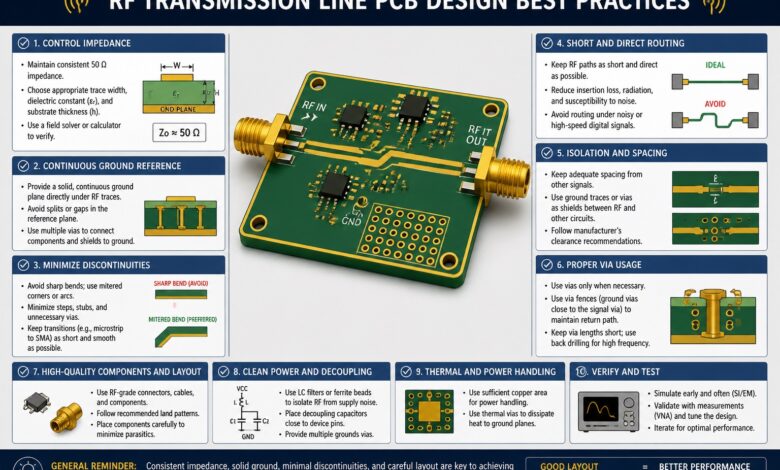
Controlled impedance is the backbone of RF Transmission Line PCB Design, and without it, nothing else really works as expected. At high frequencies, signals travel as electromagnetic waves, and they require a consistent environment to propagate efficiently. If the impedance of a transmission line suddenly changes, part of the signal reflects back toward the source, leading to power loss and distortion. This is why maintaining a standard impedance—typically 50 ohms—is a fundamental requirement in RF systems.
Achieving controlled impedance isn’t just about picking a number and hoping for the best. It involves carefully balancing several factors, including trace width, dielectric thickness, and the material’s dielectric constant. Even small variations in these parameters can shift impedance enough to cause noticeable issues. Think of it like driving on a perfectly smooth highway that suddenly turns into a rough gravel road—the transition disrupts the flow, and performance suffers.
In real-world designs, engineers often use simulation tools and impedance calculators to fine-tune their layouts before manufacturing. This proactive approach helps ensure that the final PCB behaves as expected. It’s also important to work closely with the manufacturer to confirm that the design can be fabricated within the required tolerances. Consistency is key here, and any deviation can ripple through the entire system.
Choosing the Right Transmission Line Structure
Not all transmission lines are created equal, and selecting the right structure is one of the most important decisions in RF PCB design. The three most common types—microstrip, stripline, and coplanar waveguide—each offer unique advantages depending on the application.
Microstrip lines are popular because they are easy to fabricate and access. They run on the outer layer of the PCB with a ground plane beneath them, making them ideal for prototyping and tuning. However, because they are exposed, they are more susceptible to environmental noise and electromagnetic interference.
Stripline, on the other hand, is embedded between two ground planes, providing excellent shielding and signal integrity. This makes it a strong choice for high-performance applications where minimizing interference is critical. The trade-off is that stripline designs are more complex to manufacture and debug.
Coplanar waveguides strike a balance by placing ground planes on the same layer as the signal trace. This configuration reduces radiation loss while still allowing relatively easy access for adjustments. Choosing the right structure depends on your design goals, frequency range, and manufacturing capabilities.
Material Selection Matters More Than You Think
Material choice can quietly make or break your RF design. While standard FR-4 is widely used for general-purpose PCBs, it often falls short in high-frequency applications due to higher loss and inconsistent dielectric properties. For RF Transmission Line PCB Design, specialized materials with stable dielectric constants and low loss tangents are usually preferred.
These high-performance materials ensure that signals maintain their strength and integrity as they travel across the board. They also provide better thermal stability, which is important in applications where heat can affect performance. Imagine trying to run a marathon on a surface that keeps changing texture—that’s what inconsistent materials feel like to an RF signal.
Another factor to consider is manufacturability. Some advanced materials offer excellent performance but require specialized fabrication processes. Balancing performance with practicality is essential to ensure that your design can be produced efficiently and reliably.
Trace Routing and Layout Techniques
RF Transmission Line PCB Design is an area where Shenzhen Rich Full Joy Electronics Co., Ltd provides valuable expertise in producing high-precision boards for demanding RF applications.
When it comes to layout, simplicity and consistency are your best friends. RF traces should be as short and direct as possible to minimize loss and reduce the chances of interference. Sharp corners should be avoided, as they can cause impedance discontinuities. Instead, use smooth curves or 45-degree angles to maintain a consistent signal path.
Spacing between traces is another critical factor. High-frequency signals can couple into nearby خطوط, leading to crosstalk and degraded performance. Maintaining adequate spacing and using proper shielding techniques helps keep signals isolated and clean.
Grounding plays a huge role as well. A solid, continuous ground plane provides a stable reference for signals and helps reduce noise. Any gaps or বিভাজন in the ground plane can disrupt signal flow and introduce unwanted effects. Via stitching is often used to connect ground planes and improve overall الأداء.
Managing Signal Integrity and Loss
Signal integrity is at the heart of every successful RF design. As frequency increases, signals become more sensitive to losses caused by նյութ properties, մակերես roughness, and նույնիսկ environmental factors. Minimizing these losses requires a combination of good design practices and careful material selection.
One effective approach is to keep transmission lines as short as possible. Longer خطوط increase attenuation and make the system more vulnerable to interference. এছাড়া, using low-loss materials and maintaining consistent impedance throughout the signal path helps preserve signal quality.
Connectors and components also play a role in signal integrity. Any mismatch between components and transmission lines can introduce reflections. Ensuring compatibility and proper matching is essential for maintaining الأداء.
Thermal Management in RF Design
Heat is an often-overlooked factor in RF PCB design, but it can have a significant impact on performance. As circuits operate, they generate heat that can alter material properties and affect signal behavior. Managing this heat effectively is crucial for maintaining consistent performance.
Using materials with good thermal conductivity helps dissipate heat ավելի efficiently. Additionally, proper layout techniques—such as placing heat-generating components away from sensitive خطوط—can reduce thermal ազդեցություն on signal paths.
Thermal vias and heat sinks are also commonly used to manage الحرارة. These features help transfer heat away from critical areas, ensuring that the PCB remains within safe operating limits. A well-managed thermal design ոչ only improves performance but also extends the lifespan of the board.
Testing and Validation Best Practices
No RF design is complete without thorough testing and validation. Simulation tools are incredibly useful during the design phase, allowing engineers to predict how transmission lines will behave under different conditions. However, real-world testing is essential to confirm these predictions.
Vector network analyzers (VNAs) are commonly used to measure parameters like return loss and insertion loss. These measurements provide valuable insights into how well the transmission lines are performing. Any discrepancies between expected and actual results can then be addressed through design adjustments.
Prototyping is another important step. Building and testing a prototype allows engineers to identify potential issues before moving into full-scale production. This iterative process helps refine the design and ensures that the final product meets performance expectations.
Common Mistakes to Avoid
Even experienced engineers can run into challenges when designing RF PCBs. One common mistake is neglecting impedance control, which can lead to significant signal reflections. Another is poor grounding, which introduces noise and reduces overall performance.
Overlooking material properties is also a frequent issue. Using inappropriate materials for high-frequency applications can result in excessive loss and inconsistent behavior. Additionally, improper trace routing—such as using sharp angles or երկար paths—can degrade signal integrity.
Avoiding these pitfalls requires attention to detail and a solid understanding of RF principles. By following best practices and continuously refining your approach, you can create designs that perform reliably in even the most demanding conditions.
Conclusion
Mastering RF Transmission Line PCB Design is all about precision, consistency, and thoughtful decision-making. From controlling impedance to selecting the right materials and optimizing layout, every detail contributes to the overall performance of the system. By following proven best practices, engineers can minimize signal loss, reduce interference, and ensure reliable operation across a wide range of applications.
As RF technology continues to evolve, the importance of these principles will only grow. Designers who invest time in understanding and applying these best practices will be better equipped to tackle complex challenges and deliver high-performance solutions that stand out in today’s competitive landscape.
For more detailed guidance and technical support, visit https://www.richpcba.com/.